Quantum Well Nanowire Array Micro-LEDs: The Future of On-chip Optical Communication
TOPICS: Nanotechnology Nanowires Optoelectronics
By COMPUSCRIPT LTD SEPTEMBER 17, 2023

Researchers have highlighted the potential of on-chip nanophotonic systems as a solution to the challenges presented by traditional electrical networks. These systems utilize light for data transmission, offering increased bandwidth and speed.
A new publication from Opto-Electronic Science overviews multiwavelength high-speed quantum well nanowire array micro-LED for next-generation on-chip optical communication.
As the number of cores in a processor continues to grow, so too does the challenge of connecting them all together. Traditional electrical networks fall short due to latency, limited bandwidth, and high power consumption.
Researchers have long sought a better alternative, and on-chip nanophotonic systems have emerged as a promising substitute for traditional electrical networks. On-chip optical networks utilize light for data transmission, offering great advantages over electrical signals. Light, being faster than electricity, can carry larger amounts of data through multiplexing technologies.
Key to on-chip optical networks are miniaturized light sources such as micro-/nano-scale lasers or light-emitting diodes (LEDs). However, most developments on micro-/nano-LEDs are based on III-nitride material systems at visible wavelengths. There have been limited reports on high-speed infrared micro-LEDs at telecommunication wavelengths, indispensable for the future development of Li-Fi technology, photonic integrated circuits (PICs), and biological applications.
Epitaxial grown In(Ga)As(P)/InP nanowires hold great potential for miniaturized LEDs and lasers at telecommunication wavelength range, as their wide bandgap tunability could enable monolithic integration of multi-wavelength light sources on a single chip through a single epitaxial growth, which could boost the data transmission capacity by wavelength division multiplexing and multiple-input multiple-output technologies.
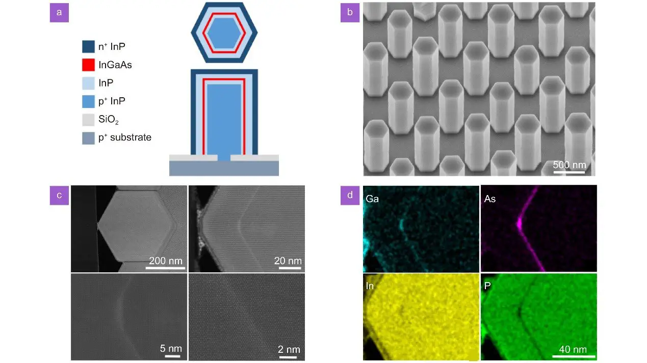
Figure 1. (a) Schematic of p-i-n InGaAs/InP single QW nanowire LED structure with lateral and vertical cross-sections. (b) 30° tilted view SEM image of the nanowire array with a pitch of 800 nm. (c) Cross-sectional HAADF-STEM image of a nanowire showing the hexagonal shape and radial QW under different magnifications. (d) EDX elemental maps of the cross-sectional region in (c). Credit: OES
Research Findings and Demonstrations
The authors of this article demonstrate the selective-area growth and fabrication of highly uniform p-i-n core-shell InGaAs/InP single quantum well (QW) nanowire array LEDs. Figure 1 (a, b) shows the schematic of the QW LED structure in a single nanowire and a scanning electron microscope (SEM) image of a nanowire array with highly uniform morphology, respectively. The detailed QW structure in the radial direction is further revealed by the high-angle annular dark-field scanning transmission electron microscopy (HAADF-STEM) image in Figure 1(c). To probe the material composition of the QW, the energy dispersive X-ray spectroscopy analysis in Figure 1(d) was also performed, clearly showing that the InGaAs QW region is gallium- and arsenic-rich compared to the InP barrier region.
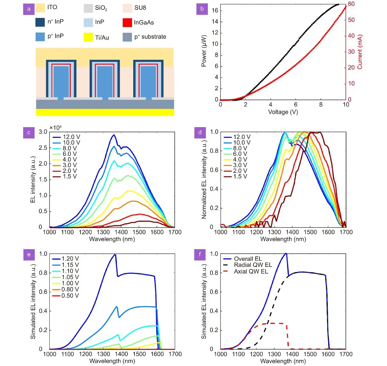
Figure 2. (a) Schematic of fabricated nanowire array LED. (b) L-I and I-V curves of a representative nanowire array LED. (c) Voltage-dependent EL spectra at room temperature. (d) Normalized voltage-dependent EL spectra from (c). (e) Simulated voltage-dependent spontaneous emission spectra. (f) Simulated emission spectrum at the bias of 1.2 V, showing the decoupled contribution from axial and radial quantum wells. Credit: OES
The QW nanowire LEDs exhibited strong bias-dependent electroluminescence (EL), shown in Figure 2 (c, d), covering telecommunication wavelengths (1.35~1.6 μm). Two prominent EL peaks can be identified from the spectra shown in Figure 2(d), including a long wavelength peak at ~1.5 μm originating from the radial QW and a short wavelength peak at ~1.35 μm due to a combined emission from axial and radial QWs.
to the presence of two EL peaks, the full width at half-maximum of the EL spectrum could reach around 286 nm, showing great promise for optical coherence tomography and bio-sensing applications. With the increased bias, large carrier injection fills the energy bands in both QWs, leading to broadened emission spectra and a shift of the peak wavelength.